processes by improving yield/reliability, process capability and manufacturability. Collaborates with Yield Analysis, Device and Defect Engineers, SPPD (Si P Product Division) designers, and Process Engineers to ensure new processes and products are capable of meeting yield and reliability requirements at the time of PRQ, and setup systems that enable best balance of manufacturability and quality for Production Ramp.
Defines and establishes process flow, procedures, and required equipment to develop new devices or products. Drives improvements and solves technical problems on quality/reliability, cost, yield, process stability/capability, and productivity. Develops solutions and solves
problems utilizing formal education, experience, statistical analysis, and problem-solving methodologies / tools. Trains production/receiving engineers for transfer to high volume manufacturing.
Full time onsite required during training, estimated 6 months. After training: hybrid " work from home" to be defined by manager and employee but continued onsite will be required. Master's in engineering (Chemical, Electrical, Materials, etc. ) 1+ years of experience in semiconductor and/or Si P process technology. ~D. in Engineering (Chemical, Electrical, Materials, etc. ) 1+ years of experience in advanced data analysis (using JMP, GAJT and/or SQL), statistical process control (SPC),
and design of experiment (DOE) principles. As the world's largest chip manufacturer, Intel strives to make every facet of semiconductor manufacturing state-of-the-art -- from semiconductor process development and manufacturing, through yield improvement to packaging, final test and optimization, and world class Supply Chain and facilities support.
Employees in the Technology Development and Manufacturing Group are part of a worldwide network of design, development, manufacturing, and assembly/test facilities, all focused on utilizing the power of Moore’s Law to bring smart, connected devices to every person on Earth. All qualified applicants will receive consideration for employment without regard to race, color, religion, religious creed, interaction, national origin, ancestry, age, physical or mental disability, medical condition, genetic information, military and veteran status, marital status, pregnancy, gender, gender expression, gender identity, interactionual orientation, or any other characteristic protected by local law, regulation, or ordinance.
It consists of competitive pay, stock, bonuses, as well as, benefit programs which include health, retirement, and vacation. For more details: jobs-search. org/finance_bernalillo-c439782/photonics-process-integration-engineer-bernalillo_i1971148053
scaling generations of hybrid lasers from proof of concept to High Volume Manufacturing (HVM) products. As a III-V Process Engineer at Intel, you will be responsible for identifying, responding to, and characterizing the III-V process line, process tool and defect problems, implementing root cause solutions to those problems, and continuously improving your toolset's safety, quality, velocity, and cost performance.
Working with a team of tool, process, yield, and product engineers across different organizations to address performance and yield problems connected to III-V process line and integration to 12" Si process line. Scoping, install and qualification of new equipment as needed.
Plan and conduct experiments to help characterize process through development cycle. Engage closely with tool vendors, drive resolution to any process and/or equipment problems methodically.
Support HVM production through on-call rotations and sustaining maintenance. demonstrates a strong sense of ownership in driving projects/tasks to completion while proactively managing stakeholders and maintaining quality in results delivered. Show flexibility and drive to accommodate changing priorities and business needs by supporting development and production roles as business needs evolve. Quick learner: demonstrate ability to learn working hands-on with process and metrology equipment in a fast-paced
manufacturing environment. Full time onsite required during training, estimated 6 months.
After training: hybrid “work from home” to be defined by manager and employee but continued onsite will be required. BS, MS, or Ph D in Electrical Engineering, Material Science, Physics, Mechanical Engineering, Microelectronics Engineering, Chemical Engineering, or related degree Bachelors with 4+ yrs experience in semiconductor processing and material characterization in an academic or industrial setting, OR Master with 3+ yrs experience in semiconductor processing and material characterization in an academic or industrial setting, OR Ph D with 1+ yrs experience in semiconductor processing and material characterization in an academic or industrial setting Experience with photonics device fabrication and characterization.
~1+ years' experience working with III-V materials, process tools. ~ As the world's largest chip manufacturer, Intel strives to make every facet of semiconductor manufacturing state-of-the-art -- from semiconductor process development and manufacturing, through yield improvement to packaging, final test and optimization, and world class Supply Chain and facilities support. Employees in the Technology Development and Manufacturing Group are part of a worldwide network of design, development, manufacturing, and assembly/test facilities, all focused on utilizing the power of Moore’s Law to bring smart, connected devices to every person on Earth.
All qualified applicants will receive consideration for employment without regard to race, color, religion, religious creed, interaction, national origin, ancestry, age, physical or mental disability, medical condition, genetic information, military and veteran status, marital status, pregnancy, gender, gender expression, gender identity, interactionual orientation, or any other characteristic protected by local law, regulation, or ordinance.
It consists of competitive pay, stock, bonuses, as well as, benefit programs which include health, retirement, and vacation. For more details: jobs-search. org/finance_bernalillo-c439782/process-development-engineer-semiconductor-bernalillo_i1968634753
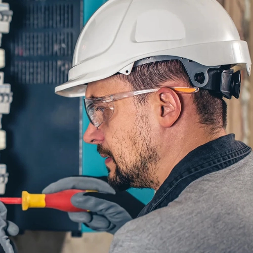
Engineering jobs encompass a broad range of careers focused on designing, developing, and maintaining structures, systems, and devices. They are characterized by a strong foundation in mathematics, physics, and technology. Engineers often specialize in fields such as civil, mechanical, electrical, or software, striving for innovation and problem-solving. These roles typically require critical thinking, collaboration, and a relentless pursuit of efficiency and functionality. Engineering careers are instrumental in shaping the future, as they constantly push the boundaries of what's possible in construction, manufacturing, communications, and various other sectors.