Location: Bernalillo, NM
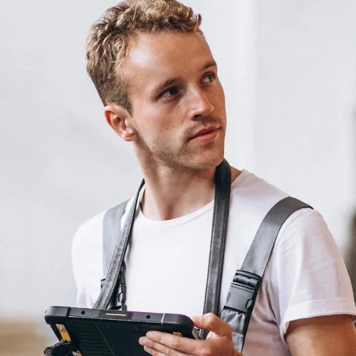
scaling generations of hybrid lasers from proof of concept to High Volume Manufacturing (HVM) products. As a III-V Process Engineer at Intel, you will be responsible for identifying, responding to, and characterizing the III-V process line, process tool and defect problems, implementing root cause solutions to those problems, and continuously improving your toolset's safety, quality, velocity, and cost performance.
Working with a team of tool, process, yield, and product engineers across different organizations to address performance and yield problems connected to III-V process line and integration to 12" Si process line. Scoping, install and qualification of new equipment as needed.
Plan and conduct experiments to help characterize process through development cycle. Engage closely with tool vendors, drive resolution to any process and/or equipment problems methodically.
Support HVM production through on-call rotations and sustaining maintenance. demonstrates a strong sense of ownership in driving projects/tasks to completion while proactively managing stakeholders and maintaining quality in results delivered. Show flexibility and drive to accommodate changing priorities and business needs by supporting development and production roles as business needs evolve. Quick learner: demonstrate ability to learn working hands-on with process and metrology equipment in a fast-paced
manufacturing environment. Full time onsite required during training, estimated 6 months.
After training: hybrid “work from home” to be defined by manager and employee but continued onsite will be required. BS, MS, or Ph D in Electrical Engineering, Material Science, Physics, Mechanical Engineering, Microelectronics Engineering, Chemical Engineering, or related degree Bachelors with 4+ yrs experience in semiconductor processing and material characterization in an academic or industrial setting, OR Master with 3+ yrs experience in semiconductor processing and material characterization in an academic or industrial setting, OR Ph D with 1+ yrs experience in semiconductor processing and material characterization in an academic or industrial setting Experience with photonics device fabrication and characterization.
~1+ years' experience working with III-V materials, process tools. ~ As the world's largest chip manufacturer, Intel strives to make every facet of semiconductor manufacturing state-of-the-art -- from semiconductor process development and manufacturing, through yield improvement to packaging, final test and optimization, and world class Supply Chain and facilities support. Employees in the Technology Development and Manufacturing Group are part of a worldwide network of design, development, manufacturing, and assembly/test facilities, all focused on utilizing the power of Moore’s Law to bring smart, connected devices to every person on Earth.
All qualified applicants will receive consideration for employment without regard to race, color, religion, religious creed, interaction, national origin, ancestry, age, physical or mental disability, medical condition, genetic information, military and veteran status, marital status, pregnancy, gender, gender expression, gender identity, interactionual orientation, or any other characteristic protected by local law, regulation, or ordinance.
It consists of competitive pay, stock, bonuses, as well as, benefit programs which include health, retirement, and vacation. For more details: jobs-search. org/finance_bernalillo-c439782/process-development-engineer-semiconductor-bernalillo_i1968634753
processes by improving yield/reliability, process capability and manufacturability. Collaborates with Yield Analysis, Device and Defect Engineers, SPPD (Si P Product Division) designers, and Process Engineers to ensure new processes and products are capable of meeting yield and reliability requirements at the time of PRQ, and setup systems that enable best balance of manufacturability and quality for Production Ramp.
Defines and establishes process flow, procedures, and required equipment to develop new devices or products. Drives improvements and solves technical problems on quality/reliability, cost, yield, process stability/capability, and productivity. Develops solutions and solves
problems utilizing formal education, experience, statistical analysis, and problem-solving methodologies / tools. Trains production/receiving engineers for transfer to high volume manufacturing.
Full time onsite required during training, estimated 6 months. After training: hybrid " work from home" to be defined by manager and employee but continued onsite will be required. Master's in engineering (Chemical, Electrical, Materials, etc. ) 1+ years of experience in semiconductor and/or Si P process technology. ~D. in Engineering (Chemical, Electrical, Materials, etc. ) 1+ years of experience in advanced data analysis (using JMP, GAJT and/or SQL), statistical process control (SPC),
and design of experiment (DOE) principles. As the world's largest chip manufacturer, Intel strives to make every facet of semiconductor manufacturing state-of-the-art -- from semiconductor process development and manufacturing, through yield improvement to packaging, final test and optimization, and world class Supply Chain and facilities support.
Employees in the Technology Development and Manufacturing Group are part of a worldwide network of design, development, manufacturing, and assembly/test facilities, all focused on utilizing the power of Moore’s Law to bring smart, connected devices to every person on Earth. All qualified applicants will receive consideration for employment without regard to race, color, religion, religious creed, interaction, national origin, ancestry, age, physical or mental disability, medical condition, genetic information, military and veteran status, marital status, pregnancy, gender, gender expression, gender identity, interactionual orientation, or any other characteristic protected by local law, regulation, or ordinance.
It consists of competitive pay, stock, bonuses, as well as, benefit programs which include health, retirement, and vacation. For more details: jobs-search. org/finance_bernalillo-c439782/photonics-process-integration-engineer-bernalillo_i1971148053
Engineering jobs encompass a broad range of careers focused on designing, developing, and maintaining structures, systems, and devices. They are characterized by a strong foundation in mathematics, physics, and technology. Engineers often specialize in fields such as civil, mechanical, electrical, or software, striving for innovation and problem-solving. These roles typically require critical thinking, collaboration, and a relentless pursuit of efficiency and functionality. Engineering careers are instrumental in shaping the future, as they constantly push the boundaries of what's possible in construction, manufacturing, communications, and various other sectors.
Performs basic well production analysis and repair of AL equipment and tests, splices, and repairs cable.. Complies with all applicable safety and environmental procedures and regulations. Ensures compliance with Health, Safety, and Environmental (HSE) regulations and guidelines.
Train and mentor lower-level technicians at the well site. RESPONSIBILITIES 3 years of experience in the oil and gas industry Basic knowledge of SCADA platforms Basic knowledge troubleshooting and repairing artificial lift equipment (POCs, Plunger controllers, etc. ) Mechanically inclined and organized Good written and verbal communication Understanding of well optimization techniques and theories Ability to multitask #woodpermian
Freeport-Mc Mo Ran is one of the world’s largest publicly traded copper producers, the world’s largest producer of molybdenum and a significant gold producer. We have a long and successful history of conducting our business in a safe, highly efficient and socially-responsible manner.
We have the assets, the talent, the drive and the financial strength to provide attractive and rewarding careers of our employees. We encourage you to take the time to explore the opportunity to advance your career at Freeport-Mc Mo Ran. Description Under general supervision, provide Geotechnical Engineering support and project management related to design, construction, and operation of ore leach pads, tailings
impoundments, storm water ponds, mining infrastructure foundations, etc. Serve as company resource for Geotechnical information and analysis. Lead in-the-field effort on site reconnaissance, geologic mapping, geotechnical drilling, geotechnical profiling, geotechnical instrumentation, construction Quality Control (QC) and Quality Assurance (QA) activities for design and construction of tailings embankments, ore leach stockpiles, foundations, and/or other mining infrastructure Lead design and construction projects related to Geotechnical data collection, analysis, and design Lead lower level Engineers and Contractors for Geotechnical project delivery Proactively seek improvements to the safe and
geotechnically stable construction and operation of ore leach pads, tailings storage facilities, storm water ponds, etc.
Assist with the development, maintenance and implementations of strategic plans to enhance mining operations' slope stability program Communicate accurate, timely and relevant Geotechnical information to operational management team and staff Perform other duties as assigned Qualifications Minimum Qualifications Bachelor's degree in Geotechnical Engineering or related Engineering discipline from an accredited curriculum, with courses in Soil Mechanics and Foundation Engineering and five (5) years of experience in an applicable field of expertise; OR Master's degree in Geotechnical Engineering or related Engineering discipline from an accredited curriculum, with courses in Soil Mechanics and Foundation Engineering and three (3) years of experience in an applicable field of expertise Knowledge in the principles and practices of Civil, Geologic, Geotechnical, or Hydrologic Engineering or a related field of Science or Engineering Knowledge of appropriate software (MS Office, Auto CAD) and Geotechnical data analysis Professional Engineer license Ability to communicate effectively, both verbally and in writing to a diversely educated audience Ability to develop and maintain awareness of occupational hazards and safety of yourself and others Skilled in following safety practices and recognizing hazards Preferred Master's degree in a related Engineering discipline Professional Engineer (PE) Certification Active tailings deposition experience including planning and execution process and/or earth embankment construction monitoring and quality assurance Experience with Geotechnical slope stability instrumentation and monitoring programs, data management and analysis Experience reviewing and editing Geotechnical engineering reports and documents for a variety of applications Engineering experience in Geotechnical analysis including field investigations, lab testing, soil characterization, slope stability and seismic analysis Experience in surface water hydrology, hydraulics and groundwater hydrology in addition to Geotechnical experience Criteria/Conditions Ability to understand and apply verbal and written work and safety-related instructions and procedures given in English Ability to communicate in English with respect to job assignments, job procedures, and applicable safety standards Must be able to work in a potentially stressful environment While performing the duties of this job, the employee is regularly required to stand, sit, demonstrate manual dexterity and work on elevated platforms Occasionally may be required to lift moderately heavy objects (up to 30 pounds) during the course of the workday Personal protective equipment is required when performing work in a mine, outdoor, manufacturing or plant environment, including hard hat, hearing protection, safety glasses, safety footwear, and as needed, respirator, rubber steel-toe boots, protective clothing, gloves and any other protective equipment as required Personal protective equipment is required when performing work in a mine, outdoor, manufacturing or plant environment, including hard hat, hearing protection, safety glasses, safety footwear, and as needed, respirator, rubber steel-toe boots, protective clothing, gloves and any other protective equipment as required Freeport-Mc Mo Ran promotes a drug/alcohol-free work environment through the use of mandatory pre-employment drug testing and on-going random drug testing as allowed by applicable State laws At Freeport, we are committed to providing an employment package that recognizes excellence, rewards value and impact, and encourages safe production.
Benefits and compensation are foundational elements of this package, along with career development opportunities, job progression and a culture supported by our core values, among others. Learn more at: FCX Jobs - Working Here Benefits: We provide an industry-leading benefits package with some of the lowest cost to employees – offering health, wellness, life insurance, paid time off, retirement savings and more. These benefits are available to you and your dependents starting day one. Our comprehensive benefits program is important to how we support the health and wellness of employees and their families.
For further benefits information please click here: Benefits Details Compensation: The estimated annual pay range for this role is currently $94,000-$132,000. This range reflects base salary only and does not include bonus payments, benefits or retirement contributions. Actual base pay is determined by experience, qualifications, skills and other job-related factors. This role is eligible for additional discretionary and incentive payment considerations based on company and individual performance.
More details will be shared during the hiring process. To view an example of a Total Rewards Estimate for this role click here: Total Rewards Estimate Safety / Work Conditions: Candidates will be required to participate in a post-offer, pre-employment medical examination for the following positions which may have essential job duties that can impact both their own safety and the safety of others: Site-based positions, or positions which require unescorted access to site-based operational areas, which are held by employees who are required to receive MSHA, OSHA, DOT, HAZWOPER and/or Hazard Recognition Training; or Positions which are held by employees who operate equipment, machinery or motor vehicles in furtherance of performing the essential functions of their job duties, including operating motor vehicles while on Company business or travel (for this purpose “motor vehicles” includes Company owned or leased motor vehicles and personal motor vehicles used by employees in furtherance of Company business or while on Company travel).
Equal Opportunity Employer